Scanning Electron Microscopy

Scanning electron microscopy (SEM) is the technique of choice for observing the surface of samples at very high resolution, down to the nanometre level, even for delicate samples.

Microscopy observations can be combined with EDX (Energy Dispersive X-ray Spectrometry) analysis, which results in a map of the chemical elements on the surface.

Assests of Scanning Electron Microscopy

  • Surface morphology
  • High spatial resolution, better than optical microscopy
  • Mapping of chemical elements on the surface
  • Non-destructive observations of fragile samples
  • No coating required, unlike standard SEM

Measurements and analyses with SEM

L’expertise Novitom en microscopie électronique SEM-FEG

  • Meticulous preparation of experimental conditions, tailored to each type of sample.
  • Data analysis based on the expertise of our electron microscopy specialists.
  • Development of analysis protocols for complex samples such as biological samples, including skin and hair.
  • Customised measurement and analysis protocols.

Types of sample

  • Any solid or semi-solid material
  • Hair and related products
  • Stratum corneum and related products

Case studies using SEM, SEM-EDX or AFM microscopy

Anti-aging skincare seen through collagen fibres organisation

Anti-aging skincare seen through collagen fibres organisation

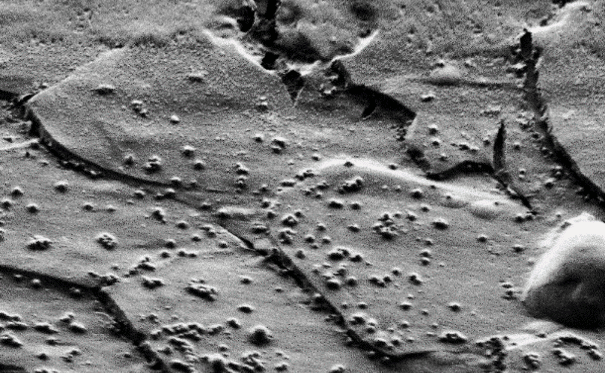
Novitom has developed an original test based on the analysis of the quality of the organisation of collagen fibres. Collagen,…

Technical characteristics for SEM and SEM-EDX

SEM-FEG

  • Voltage: 0.02 to 30 kV
  • Magnification:  12 to 1,000,000
  • Resolution: 0.8 nm at 15 kV and 2.0 nm at 1.2 kV
  • Typical acquisition time: a few seconds


EDX

  • Detectable elements: all elements with Z ≥ 6 (carbon)
  • Analysis depth in the order of μm
  • Detection limit: 0.5-2% by weight for most elements
  • Quantitative analysis: 10 to 20% maximum relative error
  • Typical acquisition time: a few minutes to tens of minutes (mapping)